On April 9, 2025, the National Medical Products Administration officially released the "Measures for the Monitoring and Evaluation of Safety Risks of Cosmetics" (hereinafter referred to as the "Measures"), marking that China's cosmetics supervision has entered a new stage of refinement and systematization, further strengthened the safety supervision of cosmetic raw materials and promoting the high-quality development of the industry. For consumers, this means that the quality and safety of cosmetics will be more effectively guaranteed. For enterprises, it is a comprehensive "physical examination" from production to circulation.
As an upstream link in the cosmetics industry chain, our raw material manufacturers will make systematic adjustments from multiple dimensions such as compliance management, technological upgrading, supply chain optimization, and risk prevention and control under the new regulations, in order to meet the requirements of the "Cosmetics Safety Risk Monitoring and Evaluation Management Measures". 1. Strengthen the safety and compliance management of raw materials, cooperate with cosmetic enterprises to complete the filing, and pay attention to dynamic regulatory requirements. Second, enhance technical capabilities and data support, and strengthen research and development innovation. Third, optimize the supply chain and traceability system, establish a full-process traceability mechanism, and strictly manage suppliers. Fourth, adjust market strategies, focus on safe, transparent and sustainable raw materials, and strengthen cooperation with downstream enterprises.
The implementation of the "Measures" will promote the cosmetics industry to develop in a safer and more transparent direction. As a key link in the industrial chain, our raw material manufacturers will proactively adapt to regulatory requirements and enhance our technological capabilities and compliance levels.
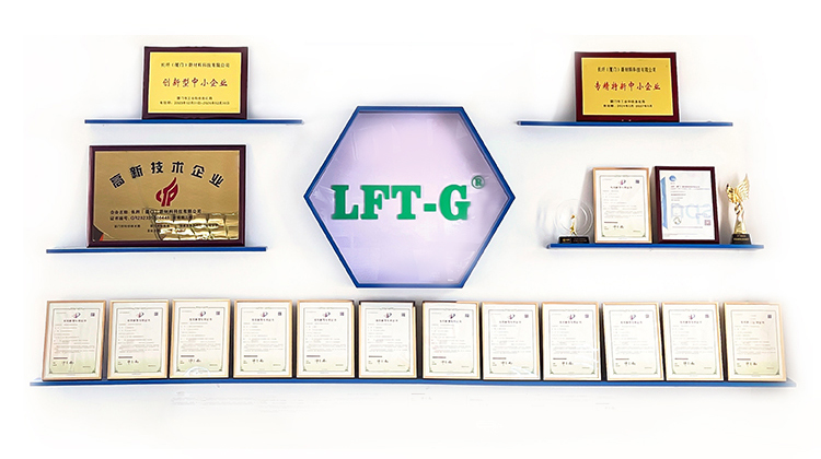
Anhui Newman Fine Chemical Co., LTD., as the top leading manufacturer of carbomer and polyacrylic acid polymers, has a sound social responsibility management policy while meeting the requirements of clean sustainable production and good quality. We pay more attention for the rights and interests of employees, improving employees' skills through various forms of training. Reduce pollution emissions, rational use of resources, to ensure that the sustainable environment standards; We, Anhui Newman always focus on customer’s request, comprehensively improve the effectiveness of the service system operation, to provide high quality, high reliability of products. Keep communication and with partners and suppliers, and employees, to promote the company to better fulfill its social responsibilities.
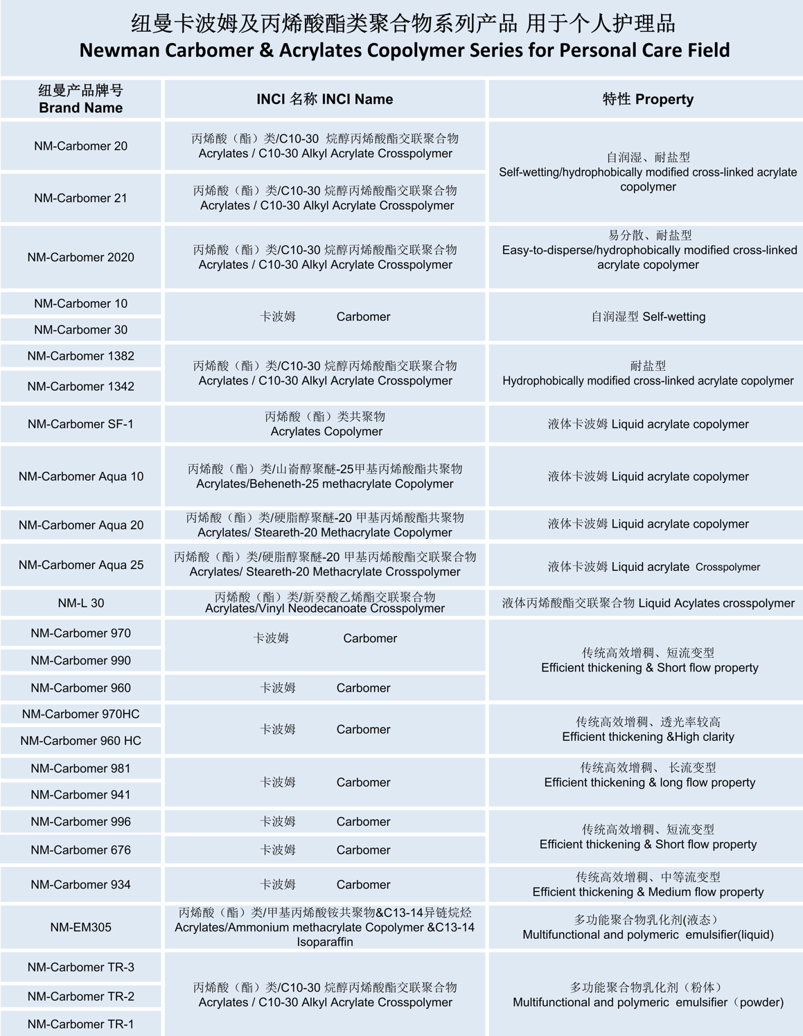
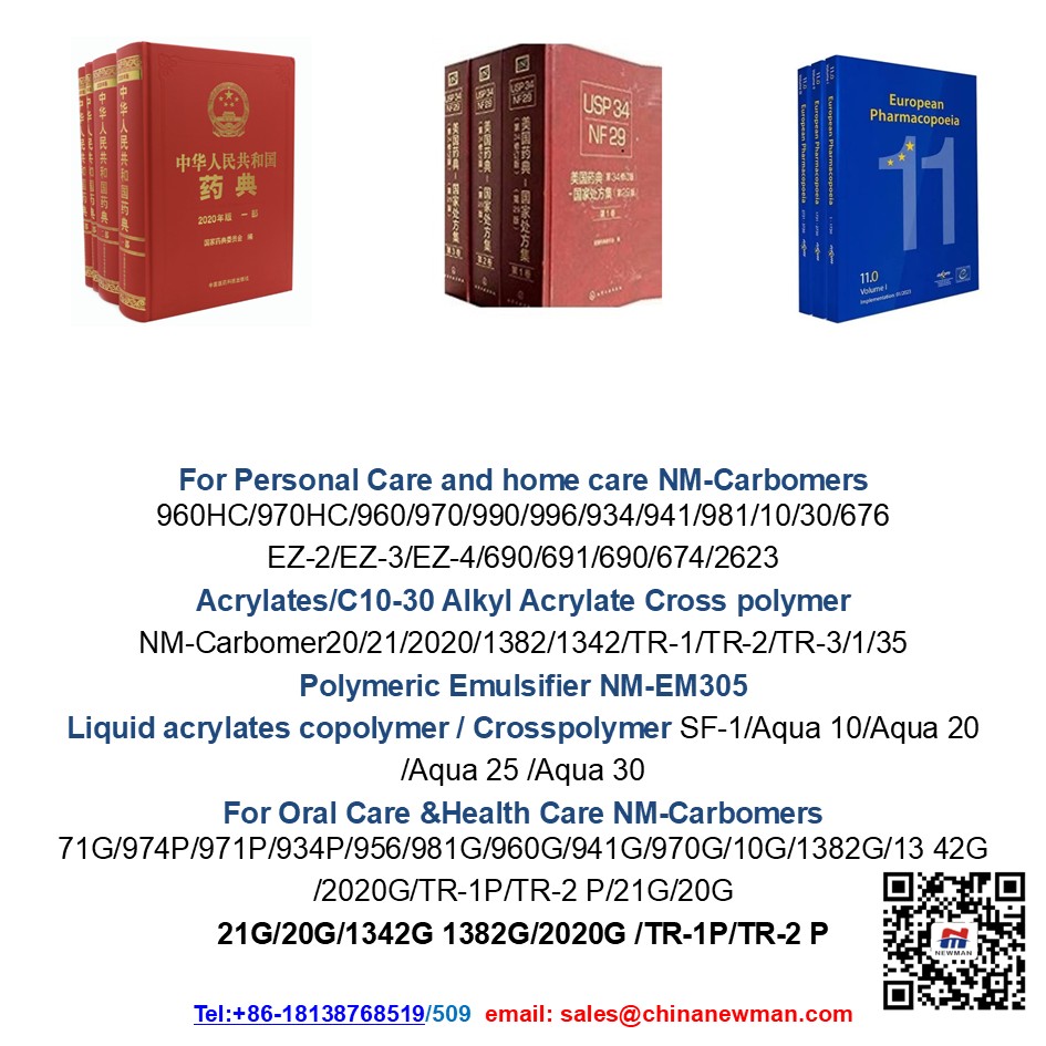
We have been engaged in strategic cooperation with the top ten customers in the global industry to launch products with Newman's characteristics. We have been launching and improving our traditional carbomer 960,970C ,996, 990 and improve carbomer 20,21,10, and 30. Especially, we launched polymeric emulsifier NM-Carbomer TR series, NM-Carbomer TR-1, TR-2 and TR-3 .And the recently best-selling general-purpose all-round rheology modifier NM-Carbomer1.
Also, we have been launching pharmaceutical grade carbomer homopolymer type A/B/C, such as NM-Carbomer 934P, 974P, 971P, 970G, and carbomer copolymer, carbomer interpolymer such as NM-Carboemr2020NF/2020G, 1382G and 10G/10NF series types. NM-Carbomers meet the requirements of major pharmacopoeia such as Chinese Pharmacopoeia 2020, USA Pharmacopoeia USP/NF, European Pharmacopoeia EP, British Pharmacopoeia BP and other relevant regulations. They have been successfully used in over the counter and pharmaceutical formulations to impart rheology modification, mucoadhesion, controlled drug release, and many other unique properties.