Application Background
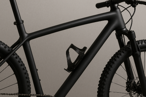
The bicycle bottle cage may look like a small accessory, but it plays an essential role.
It needs to securely hold a bottle in place on rough roads, withstand outdoor exposure to rain, temperature shifts, and UV, while still allowing smooth insertion and removal. At the same time, riders expect it to be lightweight, durable, and visually aligned with the premium image of modern carbon fiber bicycles.
Traditional solutions, such as aluminum tube cages or short glass fiber-reinforced nylon, often struggle to achieve the right balance between strength-to-weight ratio, fatigue resistance, low-temperature impact performance, and surface aesthetics.
Customer Pain Points
1. Aluminum alloy cages:
lightweight but prone to fatigue cracking and permanent deformation after repeated clamping stress and impacts; appearance mismatched with the “carbon family look” of their bicycles.
2. Short-fiber nylon cages:
low durability under moisture, heat, and cleaning chemicals; dimensional stability and clamping force decline over time; brittle failure risk in cold weather.
Target: The customer wanted lighter weight, improved fatigue and impact resistance, stable clamping force in all environments, and a carbon fiber aesthetic for premium branding.
Material Solution
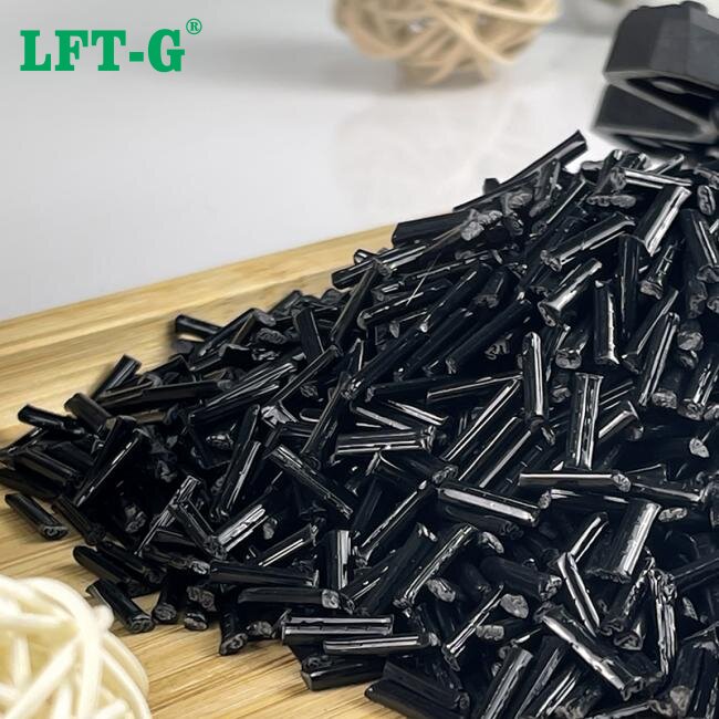
We recommended PA12 reinforced with long carbon fiber (LCF) as the optimal solution. Key advantages include:
High specific strength and stiffness: Long carbon fibers form a structural skeleton inside the polymer, providing load-bearing ability while enabling significant weight reduction.
Superior fatigue and impact resistance: The continuous fibers combined with PA12 toughness ensure long-term clamping performance even under vibration and shock.
Low moisture absorption & dimensional stability: PA12 absorbs far less water than PA6/PA66, so clamping force and bolt tightness remain consistent in wet environments.
Excellent chemical and weather resistance: Resistant to sweat, mud, cleaning agents, and road oils; ensures long-lasting performance and appearance in outdoor use.
Premium aesthetics: Natural carbon texture or controlled “fiber-floating” surface effects create a high-end, matte carbon look.
Processability: Injection moldable for mass production, ensuring dimensional consistency and cost-effectiveness at scale.
Comparison
| Solution | Weight | Impact |
Dimensional Stability |
Aesthetics |
Mass Production |
|
Aluminum Tube |
Light |
Medium |
Excellent |
Metallic |
Requires surface finishing |
|
Short-Fiber Nylon |
Medium |
Low-Medium |
Sensitive to moisture |
Generic plastic |
Moderate consistency |
|
PA12-LCF |
Lightest |
High |
Stable |
Carbon premium look |
Excellent with injection molding |
Sustainability and Compliance
Metal replacement reduces processing steps and finishing, cutting carbon footprint.
Lightweighting contributes to overall bicycle energy efficiency and performance.
Full support for RoHS, REACH, and traceability documentation as required by OEMs and brands.
Conclusion
With an experienced technical team and proven expertise in long fiber composite solutions, we help customers translate lightweight, strength, and aesthetics into a commercially viable product.
For this project, the PA12-LCF bicycle bottle cage solution not only met the customer’s technical requirements but also enhanced their premium carbon branding.
Interested in sample trials or design consultation?
Looking to extend this material platform to pedals, brake levers, derailleur hangers, or mounts?
We are ready to provide material samples, process guidelines, and validation templates to accelerate your product development.